W800-Arduino Getting Started Guide
Preparation
W800-Arduino development board
Micro USB data cable
PC (Windows, Linux, or Mac OS)
You can skip the introduction and go directly to the Application development section.
Overview
W800-Arduino is a development board from WinnerMicro based on the W800 chip.
W800-Arduino development board integrates the following peripherals:
External antenna interface and onboard antenna
Integrated 5V to 3.3V LDO chip
BOOT, RESET, and USER buttons
Built-in three-color LED light
This greatly reduces the number and cost of additional components, the complexity of assembly and testing, and increases usability.
The USER button on the W800-Arduino is provided for users to input signal detection, making it convenient for debugging related functional programs.
To facilitate the connection of more peripherals, all I/O signals and system power pins on the W800-Arduino are led out through the pins on the top and bottom of the development board, allowing users to directly plug the W800-Arduino into other development boards or connect other peripherals with Dupont wires, greatly increasing user flexibility.
Functional Description
The main components, interfaces, and control methods of the W800-Arduino development board are as follows.
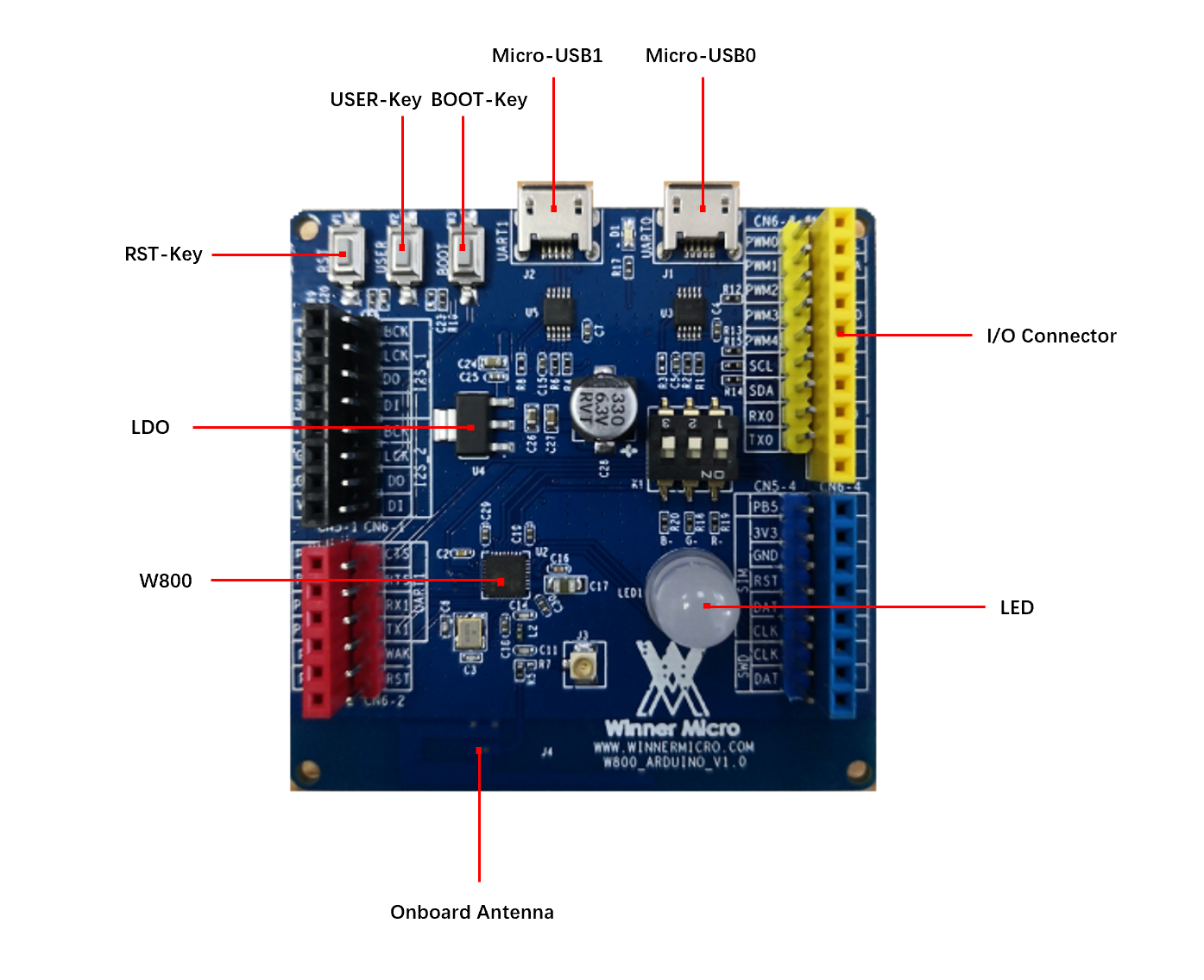
The main components of the W800-Arduino development board are described in the table below (clockwise from the top left corner).
Main Component |
Basic Description |
RST-Key |
System reset button. |
USER-Key |
User input signal detection button. |
BOOT-Key |
Download button. Press the BOOT button, then insert the USB cable into the UART0 port. Release the BOOT button to enter download mode. |
Micro-USB1 |
The other USB port on the development board has the same functionality as the default USB port. |
Micro-USB0 |
The default USB port of the development board can be used as a power supply port for the development board or as a communication interface for connecting the PC and the development board. |
I/O |
All pins of the W800 are led out to the pin headers on the development board. Users can program the W800 to achieve functions such as PWM, ADC, DAC, I2C, and I2S. For details, see 管脚说明。 |
LED |
Three-color LED for user debugging of PWM. Set the K1 switch to the ON position when using, and to the OFF position when not in use. |
Antenna |
The onboard antenna of the development board also supports external antennas. |
W800 |
The main control chip of the development board, featuring WiFi and Bluetooth. |
LDO |
5V to 3.3V LDO chip. |
Power Options
The development board can be powered by any of the following three methods:
Micro USB power supply (default). Both USB ports can be used for power supply.
5V / GND pin power supply.
3.3V / GND pin power supply.
Warning
The above power supply modes cannot be connected simultaneously, otherwise the development board or power supply may be damaged.
Pin Description
The table below introduces the name and functions of the I/O pins on the development board. For the specific layout, see the Schematic and Layout Diagram section.
Number. |
Name |
Type |
Pin Function After Reset |
Multiplexing Function |
Maximum Frequency |
Pull-up/Pull-down Capability |
Drive Capability |
1 |
PB_20 |
I/O |
UART_RX |
UART0_RX/PWM1/UART1_CTS/I²C_SCL |
10MHz |
UP/DOWN |
12mA |
2 |
PB_19 |
I/O |
UART_TX |
UART0_TX/PWM0/UART1_RTS/I²C_SDA |
10MHz |
UP/DOWN |
12mA |
3 |
WAKEUP |
I |
WAKEUP wake-up function |
DOWN |
|||
4 |
RESET |
I |
RESET reset |
UP |
|||
5 |
XTAL_OUT |
O |
External crystal output |
||||
6 |
XTAL_IN |
I |
External crystal input |
||||
7 |
AVDD33 |
P |
Chip power, 3.3V |
||||
8 |
ANT |
I/O |
RF antenna |
||||
9 |
AVDD33 |
P |
Chip power, 3.3V |
||||
10 |
AVDD33 |
P |
Chip power, 3.3V |
||||
11 |
AVDD33_AUX |
P |
Chip power, 3.3V |
||||
12 |
TEST |
I |
Test function configuration pin |
||||
13 |
BOOTMODE |
I/O |
BOOTMODE |
I²S_MCLK/LSPI_CS/PWM2/I²S_DO |
20MHz |
UP/DOWN |
12mA |
14 |
PA_1 |
I/O |
JTAG_CK |
JTAG_CK/I²C_SCL/PWM3/I²S_LRCK/ADC0 |
20MHz |
UP/DOWN |
12mA |
15 |
PA_4 |
I/O |
JTAG_SWO |
JTAG_SWO/I²C_SDA/PWM4/I²S_BCK/ADC1 |
20MHz |
UP/DOWN |
12mA |
16 |
PA_7 |
I/O |
GPIO, input, high resistance |
PWM4/LSPI_MOSI/I²S_MCK/I²S_DI /Touch0 |
20MHz |
UP/DOWN |
12mA |
17 |
VDD33IO |
P |
IO power, 3.3V |
||||
18 |
PB_0 |
I/O |
GPIO, input, high resistance |
PWM0/LSPI_MISO/UART3_TX/PSRAM_CK/Touch3 |
80MHz |
UP/DOWN |
12mA |
19 |
PB_1 |
I/O |
GPIO, input, high resistance |
PWM1/LSPI_CK/UART3_RX/PSRAM_CS/Touch4 |
80MHz |
UP/DOWN |
12mA |
20 |
PB_2 |
I/O |
GPIO, input, high resistance |
PWM2/LSPI_CK/UART2_TX/PSRAM_D0/Touch5 |
80MHz |
UP/DOWN |
12mA |
21 |
PB_3 |
I/O |
GPIO, input, high resistance |
PWM3/LSPI_MISO/UART2_RX/PSRAM_D1/Touch6 |
80MHz |
UP/DOWN |
12mA |
22 |
PB_4 |
I/O |
GPIO, input, high resistance |
LSPI_CS/UART2_RTS/UART4_TX/PSRAM_D2/Touch7 |
80MHz |
UP/DOWN |
12mA |
23 |
PB_5 |
I/O |
GPIO, input, high resistance |
LSPI_MOSI/UART2_CTS/UART4_RX/PSARM_D3/Touch8 |
80MHz |
UP/DOWN |
12mA |
24 |
VDD33IO |
P |
IO power, 3.3V |
||||
25 |
CAP |
I |
External capacitor, 4.7µF |
||||
26 |
PB_6 |
I/O |
GPIO, input, high resistance |
UART1_TX/MMC_CLK/HSPI_CK/SDIO_CK/Touch9 |
50MHz |
UP/DOWN |
12mA |
27 |
PB_7 |
I/O |
GPIO, input, high resistance |
UART1_RX/MMC_CMD/HSPI_INT/SDIO_CMD/Touch10 |
50MHz |
UP/DOWN |
12mA |
28 |
PB_8 |
I/O |
GPIO, input, high resistance |
I²S_BCK/MMC_D0/PWM_BREAK/SDIO_D0/Touch11 |
50MHz |
UP/DOWN |
12mA |
29 |
PB_9 |
I/O |
GPIO, input, high resistance |
I²S_LRCK/MMC_D1/HSPI_CS/SDIO_D1/Touch12 |
50MHz |
UP/DOWN |
12mA |
30 |
PB_10 |
I/O |
GPIO, input, high resistance |
I²S_DI/MMC_D2/HSPI_DI/SDIO_D2 |
50MHz |
UP/DOWN |
12mA |
31 |
VDD33IO |
P |
IO power, 3.3V |
||||
32 |
PB_11 |
I/O |
GPIO, input, high resistance |
I²S_DO/MMC_D3/HSPI_DO/SDIO_D3 |
50MHz |
UP/DOWN |
12mA |
33 |
GND |
P |
Grounding |
Application Development
Before powering on the W800-Arduino, please ensure that the development board is intact.
Now, proceed to the Quick Start section on Setting Up the Compilation Environment to see how to set up the development environment and try flashing the sample project to your development board.
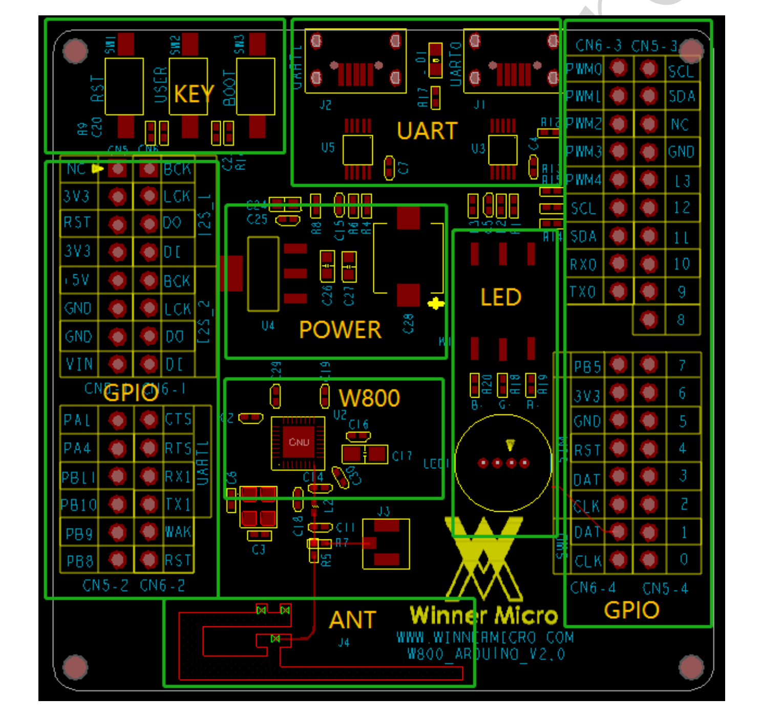
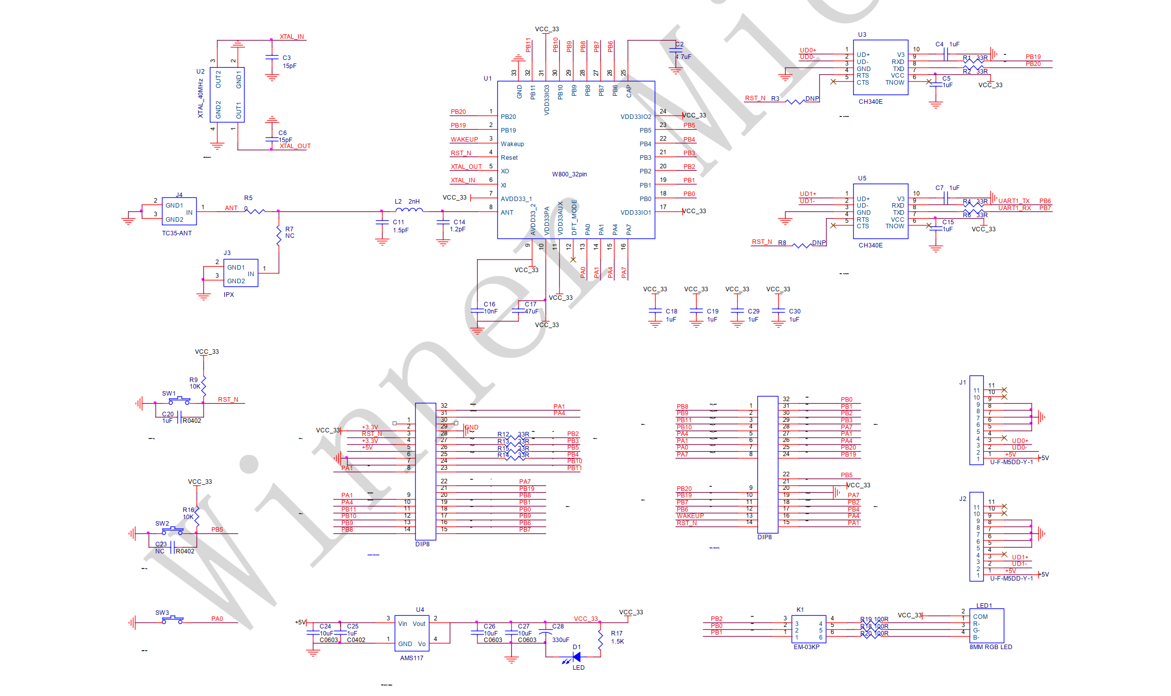
Schematic Diagram and Layout
The schematic diagram of the W800-Arduino development board is shown below.
The layout diagram of the W800-Arduino development board is shown below.